A latch will store a single binary number.
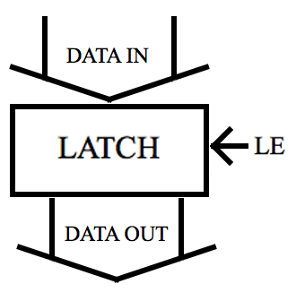
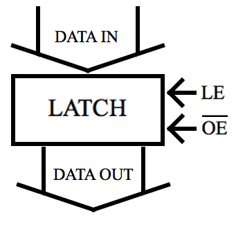
The figure above diagrams a latch that receives its input from one data bus (or address bus, or control bus) and makes it available to another. The latch in the figure has a latch enable control input. The figure below diagrams a latch that has an additional control input to enable the output. In this case, it is called the output enable bar input because its active state is logic low.
When the latch enable control input is low, the data input signals have no effect on the contents of the latch or the output of the latch. When the latch enable is high, the input data is allowed to replace the contents of the latch.
The first latch, having no output enable control, has an output which is always active. The second latch, having an output enable control, keeps its outputs off and compliant with whatever state exists on the bus attached to its outputs whenever the output enable bar control signal is high.
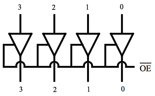
Disabling the outputs when the output enable input is in its inactive state is accomplished by means of tri-state gates. The figure above diagrams four tri-state gates that disconnect their inputs from their corresponding outputs. The bits are numbered 0 through 3.
The inputs to these tri-state gates are not the ultimate inputs of the latch. Between the latch inputs and the tri-state gates there are the elements that store the input bits.
Tri-state outputs allow many latches to have their outputs connected to the same bus so long as only one latch at a time has its output enabled. This advantage is provided to any device that has tri-state outputs (not just latches). The underlying technology does not need to be electronic. Many types of signals can be off as well as having two other possible states. Tri-state devices have three possible output states.
The figure below diagrams an enable function for a one-bit memory device that is not shown.
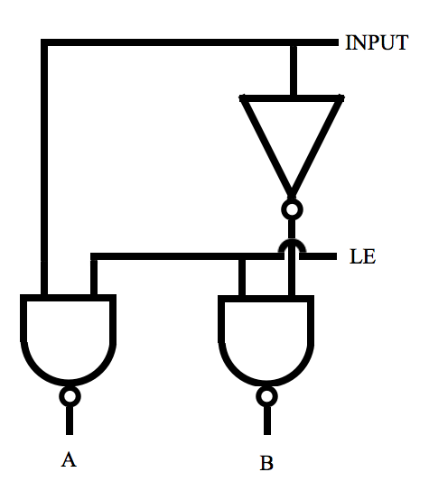
Here is its truth table:
              LE    INPUT    A      B
             -------------------------
               1      1      0      1

               1      0      1      0

               0      1      1      1

               0      0      1      1
When LE is 1, INPUT determines whether A or B is 1 while the other is 0. When LE is 0, both A and B are forced to equal 1.
The memory cell that follows is prevented from accepting a new value whenever both A and B are 1. It is updated by the INPUT whenever LE is 1.
Here is the gate arrangement that retains the bit provided by INPUT:
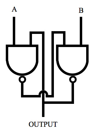
Here is its truth table:
              A      B       OUTPUT
             ----------------------
              0      1         0

              1      0         1

              1      1   Previous Output
B is the complement of A unless both A and B are 1. The LE device that precedes this assures that A and B are never both 0. When A and B are both 1, the output remains whatever it was just before A and B became both 1.
When this one-bit memory is preceded by the latch enable feature diagrammed above to control its A and B inputs, the result is called a transparent latch. The input data is transferred to the output when the LE input is a logic high, and the latch remembers the current output when LE goes to logic low.
Another type of latch is called an edge triggered latch. This latch changes its output to match the input whenever the CP (clock pulse) input goes from low to high. Only another rising edge of the CP input will change it contents.
Either type of latch may have tri-state outputs.