Microprocessor Design
Back To Introduction
Back To Introduction
The diagrams below show a half adder and a full adder.
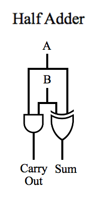
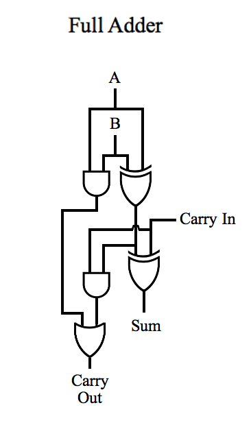
These adders add bit A to bit B, forming a sum. In order to take into account a carry in from anther adder, the full adder must combine the half adder with three additional gates. Here is the truth table for the full adder:
Carry In    B    A    Sum    Carry Out
--------------------------------------
    0       0    0     0        0
    0       0    1     1        0
    0       1    0     1        0
    0       1    1     0        1
    1       0    0     1        0
    1       0    1     0        1
    1       1    0     0        1
    1       1    1     1        1
Using subscripts, as in Cin or C0 instead of Carry In helps make the illustrations more compact. This is valuable in the case of the addition of many bits in parallel.
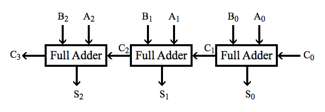
The diagram above shows three full adders used to add two 3-bit words. Each adder receives a bit from the binary word A0 through A3 and also receives a bit from the binary word B0 through B3 to produce sums S0 through S3. Because the carry input to each adder must wait for the carry output of another adder to stabilize, the propagation delays of the adders add together. This type of adder is called a ripple-carry adder. The total propagation delay from the least-significant bit to the most significant bit is unacceptable for an ALU in a 16-bit or 64-bit microprocessor.
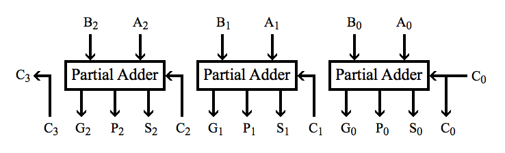
Additional logic called Carry-look-ahead logic can be used to produce all of the carry inputs essentially at the same time if each of the full adders is modified to allow the carry-look-ahead logic to provide its carry input. The gates that provide the carry output in the full adder are removed. Such an adder is shown below. The term partial full adder is sometimes used instead of the term partial adder.
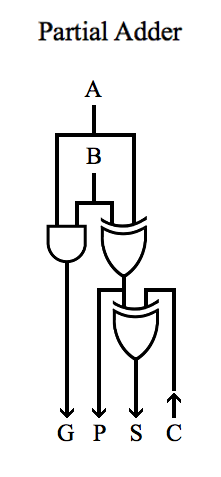
The carry input on the bottom right of the diagram will come from the carry-look-ahead logic. The sum, S, and two new outputs, P and G, are shown. The G signal is known as the carry generate signal because a carry output is generated whenever G = 1 (regardless of the carry input). The P signal is known as the carry propagate signal because whenever P =1, the carry input is to be propagated to the carry output by the carry-look-ahead logic.
Here is a diagram of a 3-bit adder that is ready for connection to a care-look-ahead logic unit:
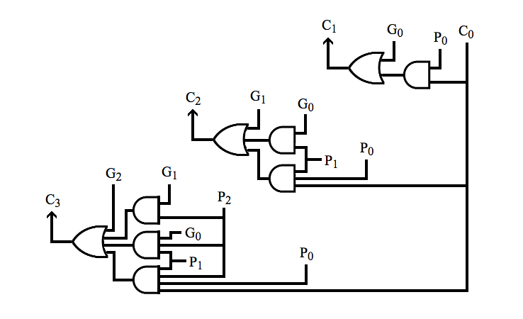
The figure above diagrams the carry-look-ahead logic. It consists of three parts. They produce C1, C2, and C3 from C0 and the P and G outputs of the partial adders. Sums S0, S1, and S2 are not used by the carry-look-ahead logic. Each of these carry signals is produced only two gate delays after any change in the C0 input.
Designing this carry-look-ahead logic and more complicated logic units by reference to truth tables alone (however well memorized) is a somewhat trail-and-error process that is tedious and prone to errors. Nothing should discourage you from becoming a virtuoso of this approach, but you should also be aware of an algebra of logic gates based on the work of George Boole. His creation is called Boolean Algebra.
Boolean algebra operates on two values. They can stand for true versus false, yes versus no, or 1 versus 0. There may be other possibilities, however, the application of Boolean algebra to logic gates for addition and other ALU functions is normally couched in terms of 1's and 0's.
Knowing the purpose and constraints associated with a desired logic-gate function, a workable arraignment can often be found by solving Boolean equations.
Early on, the symbols for AND and OR were defined this way: A AND B = A ∧ B, and A OR B = A ∨ B. Using these symbols, equations looked like this:
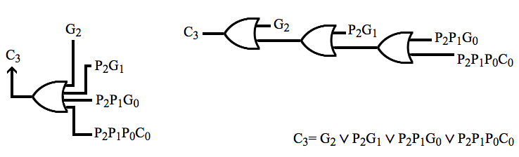
C3 = G2 ∨ P2 ∧ G1 ∨ P2 ∧ P1 ∧ C1
Motivated by greater clarity, other symbols have become popular. A AND B is often written A · B, or simply AB, indicating the multiplication of the inputs. So long as the input numbers are limited to 1 and 0, this ordinary multiplication gives the same result as an AND gate, even if that gate has more than two inputs. The result of using AB to mean A AND B seems clearer:
C3 = G2 ∨ P2G1 ∨ P2P1C1
The plus sign, used to add numbers, has become a popular substitute for the OR symbol. This makes equations look more familiar:
C3 = G2 + P2G1 + P2P1C1
Using + in place of ∨ presents a problem. 1 + 1 is not 1. Using + requires taking care to recognize two meanings for the plus symbol because its meaning depends on the context. If you are sure that the equation is Boolean, you can get away with using the plus sign; but I prefer to avoid having two context-dependent meanings for + by consistently using ∨ for OR.
The preferred symbol for XOR is ⊕, so A XOR B = A ⊕ B. With the A ⊕ B, A ∨ B, and AB logical operations we have enough to describe the partial adder and the carry-look-ahead logic.
In the partial adder, we have three equations:
P = A ⊕ B
G = AB
S = P ⊕ C
In the full adder we also have an equation for the carry output:
Cout = G ∨ PCin
In fact, this is the model for the first of three sections in the carry-look-ahead logic that produces C1. It nearly returns to the partial adder what was taken away from the full adder:
C1 = G0 ∨ P0C0
The sections for C2 and C3 must perform the same logical operations. The substitutions are key to revealing the structure of these sections:
C2 = G1 ∨ P1C1
= G1 ∨ P1(G0 ∨ P0C0) Substituting C1 with its value
= G1 ∨ P1G0 ∨ P1P0C0
C3 = G2 ∨ P2C2
= G2 ∨ P2(G1 ∨ P1C1) Substituting C2 with its value
= G2 ∨ P2G1 ∨ P2P1C1
= G2 ∨ P2G1 ∨ P2P1(G0 ∨ P0C0) Substituting C1 with its value
= G2 ∨ P2G1 ∨ P2P1G0 ∨ P2P1P0C0
We now have an equation for each of the three sections of the carry-look-ahead logic:
C1 = G0 ∨ P0C0
C2; = G1 ∨ P1G0 ∨ P1P0C0
C3= G2 ∨ P2G1 ∨ P2P1G0 ∨ P2P1P0C0
These equations can readily be translated into logic designs. Consider C3. There are four terms that need to be ORed together. This can be done serially, or it can be done by a four-input OR gate. Logically, these two ways produce the same result.
The propagation delay is much longer in the serial arrangement than in the four-input OR gate, but their truth tables are the same.
The C3 equation also clearly implies three AND gates. They are P2G1, P2P1G0, and P2P1P0C0.
The serial versions have the same truth tables as versions that use many inputs, and they have the same Boolean expressions. The serial versions have much longer propagation delays; but if the underlying technology is electronic, and they have more than just a few inputs, they have noticeably longer propagation delays. For this reason, a multilevel approach is used for 16-bit and 64-bit addition. It keeps the number of logic-gate inputs limited to four, and avoids the extra delays that would be caused by 17-input and 65-input electronic gates.
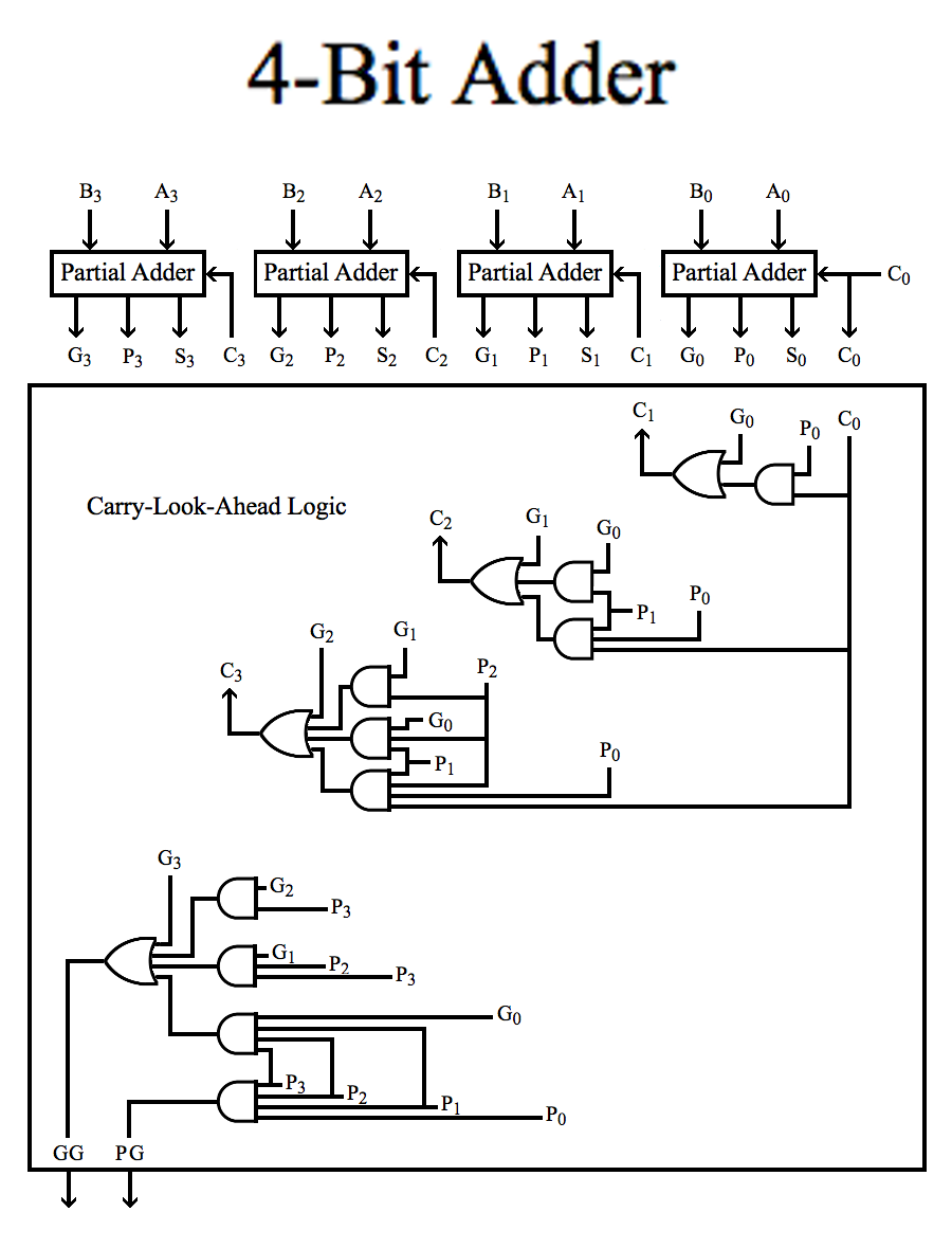
The 4-Bit adder diagramed above has a fourth partial adder and does not directly produce C4. Instead, it produces two new outputs, GG and PG. This makes wider adders possible without using gates that have more than four inputs.
The Boolean expression for PG is P3P2P1P0 and GG = G3 ∨ G2P3 ∨ G1P3P2 ∨ G0P3P2P1.
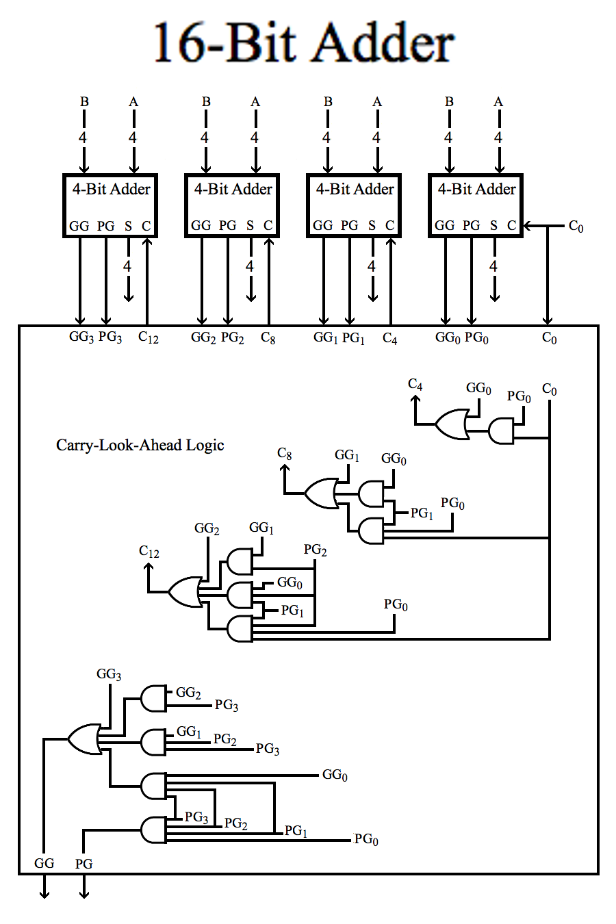
The 4-bit adder diagramed above could be substituted for any of the four 4-bit adders used in the 16-bit adder shown below. In the 16-bit adder, C4 is produced by GG0, PG0, and C0. The combined Boolean equation for the GG and PG logic above together with the logic producing C4 in the 16-bit adder is as follows:
PG0 = P3P2P1P0
GG0 = GG = G3 ∨ G2P3 ∨ G1P3P2 ∨ G0P3P2P1
C4 = GG0 ∨ PG0C0
= GG0 ∨ P3P2P1P0C0 Substituting PG0 with its value
= G3 ∨ G2P3 ∨ G1P3P2 ∨ G0P3P2P1 ∨ P3P2P1P0C0 Substituting GG0 with its value
= G3 ∨ P3(G2 ∨ G1P2 ∨ G0P2P1 ∨ P2P1P0C0) Factoring P3 out as a common factor.
= G3 ∨ P3(G2 ∨ P2 (G1 ∨ G0P1 ∨ P1P0 C0)) Factoring P2 out as a common factor.
= G3 ∨ P3(G2 ∨ P2 (G1 ∨ P1(G0 ∨ P0C0))) Factoring P1 out as a common factor.
= G3 ∨ P3(G2 ∨ P2 (G1 ∨ P1C1)) Substituting the value of C1 with C1
= G3 ∨ P3(G2 ∨ P2C2) Substituting the value of C2 with C2
= G3 ∨ P3C3 Substituting the value of C3 with C3
The pattern has been maintained while limiting the number gate inputs to four. The 16-bit adder has two levels, each with a carry-look-ahead unit.
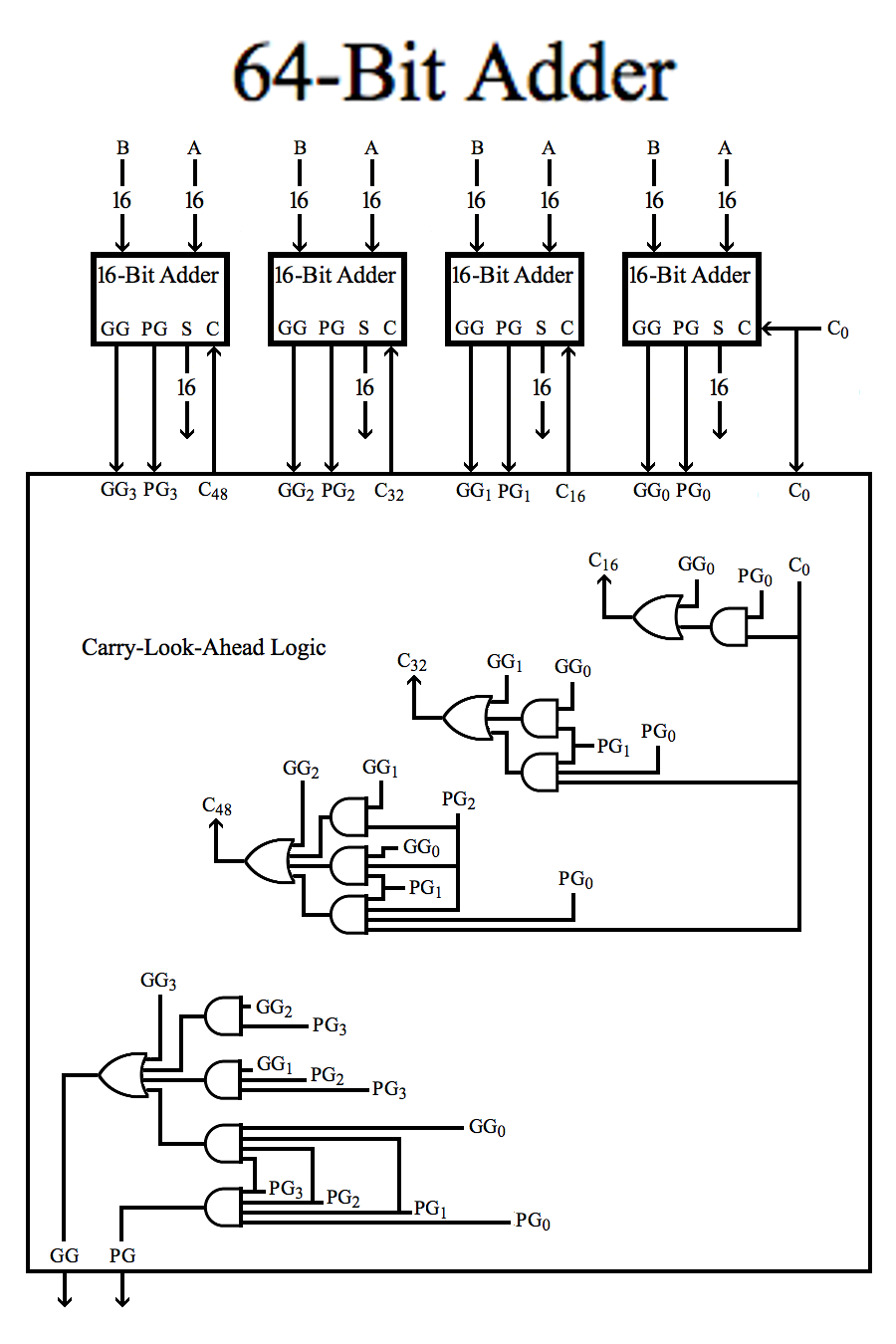
The 64-bit adder below is a three-level unit.
The carry input C0 can come from the processor status register or from a bit saved from the last carry output of the ALU.